DARPA To Develop Advanced Tiny Chip-Scale Atomic Clocks For Military PNT Applications
Defense Advanced Research Projects Agency (DARPA) is presently working on an advanced version of its first-generation, battery-powered, miniature chip-scale atomic clock (CSAC) with 1000x performance improvements for Positioning, Navigation, and Timing (PNT) applications.
DARPA’s Atomic Clock with Enhanced Stability (ACES) program aims to build the next-generation atomic clock owing to the limitations of the now commercially available CSACs.
“Today’s communications, navigation, financial transaction, distributed cloud, and defense applications rely on the precision timing of atomic clocks – or clocks that track time based on the oscillation of atoms with the highest degrees of accuracy. Harnessing the power of atoms for precise timing requires a host of sophisticated and bulky technologies that are costly to develop and consume large amounts of energy,” DARPA said in a statement Tuesday.
The CSACs offer unprecedented timing stability for their size, weight, and power (SWaP). Calibration requirements and frequency drift can generate timing errors, making it difficult to achieve the highest degrees of accuracy and reliability in a portable package, the statement read.
Through the exploration of alternative physics architectures and novel component technologies, three sets of researchers have demonstrated early progress towards creating CSACs with 1000x improvement in temperature control, aging, and retrace.
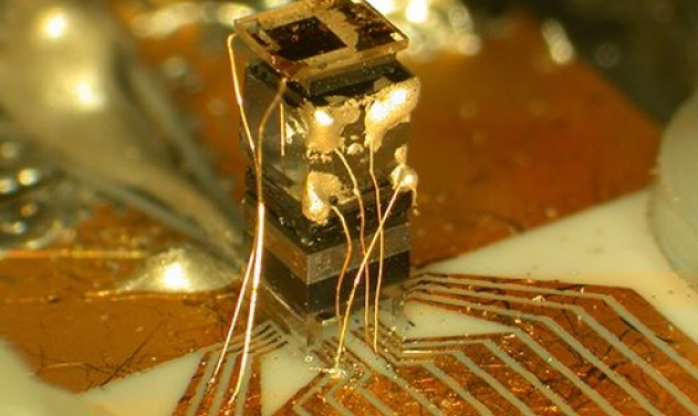
A paper recently published in Optica highlights recent progress made by a team of researchers from the National Institute of Standards and Technology (NIST), with support from researchers at the California Institute of Technology, Stanford University, and Charles Stark Draper Laboratories. The team has demonstrated an experimental optical atomic clock that is comprised of only three small chips and supporting electronics and optics. Unlike standard atom clocks that operate at microwave frequencies and track the vibrations of cesium atoms, optical atomic clocks run at higher frequencies, offering greater precision because they divide time into smaller units. The NIST team’s clock uses a laser to track the oscillations of rubidium atoms confined in a vapor cell – or tiny glass container – that is 3 millimeters across sitting on top of a silicon chip. Within the clock’s chip-based “heart,” two frequency combs act like gears to convert the rubidium atoms’ high-frequency optical “ticks” to the lower microwave frequency, which is used by most PNT applications to track time. In addition to providing a higher-degree of accuracy (roughly 50 times better than the current cesium-based CSACs), the experimental clock uses very little power – just 275 milliwatts.
A second team of researchers from Honeywell, working in partnership with University of California, Santa Barbara, is developing precision atomic sensors to support the development of a miniature atomic clock.
To date, the miniaturization of trapped-atom sensors has been stymied by bulk optical elements - such as lenses and mirrors - that traditionally compose the necessary optical system. The precision atomic sensors the Honeywell team has developed rely on a magneto-optic trap (MOT), which requires a three-dimensional arrangement of laser beams coming from different directions, precisely crossing at a point. To achieve this precise configuration without the use of lenses or mirrors, the researchers developed an integrated photonic chip that guides light around an “optical circuit” – which is analogous to the guiding of electrical signals in traditional computer chips. The photonic chip emits three large collimated beams of light in the proper three-dimensional arrangement to make a MOT. By combining these intersecting laser beams with a specialized set of compact magnetic field coils, Honeywell used this light source to trap rubidium atoms, and realize an advanced, miniature atomic clock.
Honeywell’s integrated photonic chip technology not only reduces the size, weight, and power of laser delivery systems, but also allows for batch fabrication of complex optical systems with reduced manufacturing cost.
Finally, a team from NASA’s Jet Propulsion Laboratory (JPL), with support from researchers at SRI International; University of California, Davis; and University of Illinois Urbana-Champaign, has demonstrated an experimental atomic clock capable of meeting ACES’ target metrics, while proving immune to temperature and environmental issues. Building off research that created the Deep Space Atomic Clock (DSAC), the team developed an ion-based approach to atom cooling that relies on ionized mercury and ultraviolet lamps instead of lasers. The JPL atomic clock showed an immunity of less than 1 part in 14 decimal places for 1 degree Celsius change. To put that in perspective, that is about 100x better than current CSACs. The use of mercury ions also provides more stability while making the technology less sensitive to magnetic fields and temperature changes.
Raytheon, DARPA Hypersonic Weapon Moves Closer to Development
DARPA to Develop Artificial Intelligence based Top Guns

DARPA Selects Northrop Grumman To Develop Bio Sensors To Detect Underwater Threats
Anduril to Supply $1.98 Billion Worth Counter-UAS Platforms to Kuwait

Iran Deployed Mach 9 Speed Missiles in Attacks Against Israel

Eurofighter Typhoon Jet to Become More Lethal with New Aerodynamic Modification

Tehran Claims to Have Hit Israeli Airbases in Response to Overnight Israeli...

One Month Since U.S., Israeli War Against Iran: Who Is Gaining?
One month after the United States and Israel launched coordinated strikes on Iran on February 28 the conflict has expanded...

Modern Tank Showdown: T-90MS, Leopard 2A7, M1E3 Abrams Compared
Main Battle Tanks (MBTs) have shown their mettle in recent conflicts such as in Ukraine despite being increasingly vulnerable to...

European Nations Prioritizing Europe-made IRIS-T & SAMP-T over American Patriot Air Defense Systems?
European nations looking to procure new air defense systems appear to be giving the much-vaunted American Patriot a miss in...

Russian T-90MS Crew Discuss Future Upgrades
Defense Mirror spoke with the crew members of the Russian T-90MS main battle tank, produced by UralVagonZavod

China's Mass-produced J-35A Aircraft Set to Disrupt Global Stealth Fighter Market
China is aiming to disrupt the global stealth fighter market by mass-producing its fifth-generation J-35A at a pace comparable to...

The Future of Combat: Miniaturized Laser Weapons Set to Replace Bullets and Missiles
Lasers may soon replace bullets, and drones could disable enemy UAVs with beams of light instead of missiles